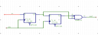
用verilog语言描述图中电路
module test (in, clk, rst_n, out);
  input in;
  input clk;
  input rst_n;
  output out;

  reg A;
  reg B;
  wire B_reg;

  always @(posedge clk or negedge rst_n)
  begin
    if(!rst_n)
      begin
          A <= 1'b0;
          B <= 1'b0;
      end
    else
      begin
          A <= B_reg;
          B <= in;
      end
  end
  assign B_reg = B;
  assign out = (~A) & B;

endmodule
已验证,有帮助望采纳!
module verilog_module
(
    input        clk,
    input        in,
    output        out
);
    reg    out_r1;
    reg    out_r2;

    always @ ( posedge clk)
    begin
        out_r1    <= in;
        out_r2    <= out_r1;
    end

    assign    out = out_r1 & (~out_r2);

endmodule